sábado, 24 de julio de 2010

Military enlists microfluidic hospital on-a-chip


The aim of a $1.6 million Office of Naval Research program is to create a microfluidic hospital on-a-chip by 2012 that can be deployed on the battlefield to monitor a soldier's injuries and administer medications. Today injured soldiers are left where they lie -- after being shot, stunned or made victims of shrapnel wounds -- until "hot zones" cool off enough for medics to reach them. But if each solider wore a hospital on-a-chip as a part of their standard-issue gear, then their condition could be assessed with microfluidic devices that harness MEMS techniques to diagnose and administer appropriate drugs to stabilize the injured soldiers’ condition until medics can reach them.


ADAN CHAPARRO
CI:17501640
EES
DIRECCION WEB: http://www.memsinvestorjournal.com/

MEMS microbots harness insect “know-how”


Microbots based on MEMS have long been sought to collect environmental samples, to search for survivors in collapsed buildings and for other reconnaissance style missions that are ill-suited for people. Although decades in the making, one major “hang-up” for fully autonomous operation of such microbots remains – a locomotion source. The tiny mechanisms and electrical circuitry are relatively easy to cast, but currently there are no reliable locomotion sources on such a small scale.


ADAN CHAPARRO
CI:17501640
EES
DIRECCION WEB: http://www.memsinvestorjournal.com/

MEMS market to propel toward double-digit growth in 2010

Powered by the seemingly recession-proof performance of the mobile phone and consumer electronics segments, the market for MEMS sensors is set to return to growth in 2010 after two straight years of decline, according to iSuppli Corp. Approaching a point close to the historical peak of 2007, MEMS revenue this year is projected to reach $6.54 billion, up 11.1 percent from $5.88 billion last year. The double-digit expansion predicted for 2010 compares to a decline of 6.8 percent posted in 2009, on top of a 3.6 percent contraction in 2008, iSuppli figures show. The market is predicted to expand through 2014, by when it is projected to grow by another $3.3 billion to hit $9.8 billion -- equivalent to an annual growth rate of 10.7 percent throughout the 2009-2014 period.


ADAN CHAPARRO
CI:17501640
EES
DIRECCION WEB: http://www.memsinvestorjournal.com/

MEMS turning mobile devices into a worldwide sensor network

U.S. Department of Homeland Security has been exploring ways to deploy sensors nationwide by riding on the existing infrastructure, such utility poles, street lights, traffic signals and government weather stations, all of which have been proposed as recipients of a nationwide deployment of MEMS sensors. The massive funding required for such a nationwide deployment has not materialized, and yet millions of MEMS sensors are being deployed in a worldwide wireless network – namely, inside laptop computers and smartphones.
Continue reading "MEMS turning mobile devices into a worldwide sensor network" »


ADAN CHAPARRO
CI:17501640
EES
DIRECCION WEB: http://www.memsinvestorjournal.com/

MEMS applications for treatment of nervous system disorders


I had recently written an article here on the use of MEMS in neuroscience research applications, and Colin Johnson penned a separate article on how MEMS are enabling systems to restore sight for the blind. This article focuses on the increasing use of MEMS for treating diseases and injuries of the central nervous system (brain and spine), including paralysis, Parkinson’s disease, and drug-resistant depression.
As background, according to Zack Lynch at the Neurotech Industry Organization, medical devices for treatment of nervous system disorders is a $7 billion market. Although small compared to the $120 billion market for neuropharmaceuticals, the neuro-device market is growing at 15% per year and is considered a real growth market, albeit one with considerable investment requirements and considerable risk.


ADAN CHAPARRO
CI:17501640
EES
DIRECCION WEB: http://www.memsinvestorjournal.com/

Mems optical


We offer custom solutions to OEM manufacturers ranging from concept to full scale volume manufacturing. Our facilities include a class 100 clean room environment, lithography and thin film processing. Our high standard of quality control is ensured by a suite of metrological systems and the use of modern statistical methods which underpin all of our production processes. As an ISO 9001:2008 certified company, we ensure the highest level of quality at a consistent level..
Axetris standard capabilities
Photolithography
Photolithography of 1 µm for up to 8" wafers
Single or double sided alignment
Thick resist processing (SU8, others)
Spray coating on severe topographies
Wet Etching
Anisotropic Silicon etching
Glass etching
Metal etching

Axetris standard capabilities
Photolithography
Photolithography of 1 µm for up to 8" wafers
Single or double sided alignment
Thick resist processing (SU8, others)
Spray coating on severe topographies
Wet Etching
Anisotropic Silicon etching
Glass etching
Metal etching
Metallization
Sputtering up to 8" wafers
Dielectric coating deposition
Silicon oxides and nitrides by PECVD
Oxides or nitrides by reactive sputtering
Reactive Ion Etching
Fused Silica
Silicon
Silicon Nitride / Oxide
Photoresist
Metrology and characterization
Interferometric and tactile surface measurements
Film thickness measurement
Resistivity & resistance
Optical microscopy
Scanning electron microscopy (SEM)
Axetris special capabilities
Micro-optics
Refractive and diffractive for micro-optical elements
Thin membranes
Thin dielectric membranes for optics, sensors and life science applications
CMOS wafers post processing
CMOS post processing like back side openings, metallization, thin film deposition


ADAN CHAPARRO
CI:17501640
EES
DIRECCION WEB: http://www.leister.com/axetris/services.htm?gclid=CIWr5vWqhaMCFRNO5QodajRWew

Plastic Optics and Plastic Molds

MEMS Optical has the capability to make high performance gray scale injection molded plastic optics and molds for injection molding of plastic optics.
High performance plastic optics are possible due to the use of our patented gray scale technology. Diffractives (beam splitters, top hat beam shapers, holograms) with efficiencies of between 75% to 90% can be achieved. Plastic refractive microlenses are also possible and they can be spherical, aspherical, torroidal, square shaped, round shaped, hexagonal, or cylindrical. This allows the inherent advantages of plastic (high-production quantities at low cost) ) to be achieved while still achieving performance far superior to binary optics.
Molds for plastic micro optics, both diffractive and refractive, can also be supplied. These molds can be delivered in a very short turn around time and in a wide variety of sizes.
As plastics become more appropriate for optics, MEMS Optical is capable of providing either the molds or the parts themselves that will make possible the products of the future.


ADAN CHAPARRO
CI:17501640
EES
DIRECCION WEB: http://www.memsoptical.com/prodserv/products/plastics.htm

mems optical fine pitchc grating

MEMS Optical also has unique equipment capable of making extremely fine pitch gratings on a wafers scale at low cost and with quick turnaround times. The image indicates a grating with a depth of 395 nm and a width of 294 nm. These gratings allow for light to be very efficiently diffracted at grazing incident angles. Useful when dense wavebands need to be separated or when large diffraction angles need to be generated, this capability opens up a range of other applications.
For example, by making the pitch smaller than the wavelength, form bi-refringence can be achieved and pixilated polarization imagers can be created as well as wafer scale retarders. Yet another application is the creation of moth's eye" type anti-reflection surface structures eliminating the need for antireflective coatings.
Applications
Wire grid and pixilated wire grid polarizers
Polarization imagers
Retarders
Pixilated polarization imagers
DWDM
Anti-reflection surfaces without the need for AR coatings


ADAN CHAPARRO
CI:17501640
EES
DIRECCION WEB: http://www.memsoptical.com/prodserv/products/finepitch.htm

Laser Diode Corrector


MEMS Optical is currently developing a laser diode corrector which can take the elliptical output beam from a laser diode and circularize it. Due to it's operating principle, it has a major advantage in that precise alignment is not required making assembly operations much simpler and faster. Due to the ability to manufacture this device in wafer scale, it can be economically manufactured and these savings can be passed on to our customers. Our laser diode corrector has less than 0.1 waves of wavefront error.


ADAN CHAPARRO
CI:17501640
EES
DIRECCION WEB: http://www.memsoptical.com/prodserv/products/laserdiode.htm

Beam Shapers


Beam Shapers
Lasers do not typically have a uniform beam profile across the entire area of their output. Beam shapers are typically used to convert a gaussian beam intensity profile to a uniform "top hat" shape. These are often the most complex optics to design but MEMS Optical's gray scale lithography allows for the creation of extremely high performance beam shapers, often with uniformity within 2% with virtually no speckle present.

Beam shapers are usually diffractives and work best with a single mode beam but, if a multimode beam is used, a refractive beam integrator type can be made.


The Images
The images here are actual measurements taken from a beam before and after it has passed through a MEMS Optical beam shaper.
Gaussian - Beam intensity profile before shaping


ADAN CHAPARRO
CI:17501640
EES
DIRECCION WEB: http://www.memsoptical.com/prodserv/products/bshapers.htm

COLLIMATOR FIBER ARRAYS

MEMS Optical Inc. has developed a proprietary process to actively align and attach our microlens arrays to precision-aligned fiber pigtails, creating collimator arrays, providing excellent beam positioning and pointing accuracy. Each collimated beam is parallel to all other beams within the array, and all emanate from the microlens array at a known fixed perpendicular angle.

MEMS Opticals' collimator arrays are available in both linear and two dimensional configurations, which allows for collimator arrays ranging from just a few to multiple hundreds. Each microlens is custom made, so our customers receive a product which specifically meets their diameter and focal length requirements.

MEMS Opticals' collimator arrays can be integrated with other arrayed components, including fibers, filters and MEMS Opticals' Series 8000 two-axis tilt mirror, also available in array configurations.

Features and Benefits

1D and 2D collimator array options

Custom microlens design

100% microlens inspection

100% collimator inspection

Custom fiber length and connector options

Pointing Accuracy +/- 0.05 degrees (typical)

Collimator to collimator insertion loss


ADAN CHAPARRO
CI:17501640
EES
DIRECCION WEB: http://www.memsoptical.com/prodserv/products/fiberarrays.htm

Microlens Arrays"


Microlens arrays are a vital part of today's optical systems. From telecommunications to machine vision, microlenses are impacting the way we live. . Now, by applying MEMS Optical’s patented gray scale production process, MEMS Optical can design and fabricate microlenses that are:

a. refractive

b. diffractive

c. anamorphic

d. aspherical

e. spherical

f. positive (convex)

g. negative (concave)

Lenses can be either refractive or diffractive and can be as small as 15 microns diameter. Using standard materials such as fused silica and silicon and newer materials such as Gallium Phosphide and Calcium Fluoride a wide variety of lenses can be made. Lenses can be made on one side with absolute alignment accuracies which allow each lens to be within 0.25 microns of it's ideal location and a front to back surface alignment capability that allows lenses on both sides of a substrate to be aligned to within 1 micron. Surface roughness values of 20 to 80 angstroms RMS are typical and the addition of AR coatings produces optics with very high transmission rates.

MEMS Optical has a full design staff capable of designing lenses for customers who don't have a design capability. Both stock and custom designs are available.
Features and Benefits
Excellent uniformity in focal length and extremely low insertion loss for 1D and large 2D array configurations

High Transmission with Low Insertion Loss (<0.5>


ADAN CHAPARRO
CI:17501640
EES
DIRECCION WEB: http://www.memsoptical.com/prodserv/products/microlensar.htm

Gray scale technology


Gray scale technology allows for the creation of a wide variety of shapes allowing for the best optical performance achievable. Traditional binary optics rely on a "stairstep" shaped approximation of the ideal surface shape. Gray scale can actually create that ideal shape. Curves, ramps, torroids, or any other shape is possible.
The pictures on this page show some of the various structures that can be created. Depending on the design, MEMS Optical can create feature sizes as small as 3 microns in gray scale and about 0.5 microns in binary products. Gray scale optics are currently being provided in production quantities to companies in fields such as Defense and Security, Telecommunication, Biomedical, Semiconductor, and Commercial Electronics, as well as other industries at lower prices than ever before. Optics such as beam splitters, diffusers, beam shapers, and microlenses are all possible with the gray scale process. Gray scale routinely provides performance far superior to binary optics and allows for the creation of optics that could not previously be fabricated.


ADAN CHAPARRO
CI:17501640
EES
DIRECCION WEB: http://www.memsoptical.com/prodserv/products/grayscale.html

Multi-function Optics

Due to the advantages of gray scale technology, multi-functional optics can now be created.
The bottom left image shows an optic that could not be made without the gray scale method. In this picture, a microlens array is shown with a grating superimposed on the lens. If a mixed red/green/blue beam is passed through the optic, the lens function will focus the beam into a spot and the grating function will separate the three component wavelengths resulting in the output seen in the bottom right image. This capability is especially attractive for projection television and increased efficiency for LCD panels.


ADAN CHAPARRO

CI:17501640

EES

DIRECCION WEB:

http://www.memsoptical.com/prodserv/products/multi-func.htm

PROYECTO "DISPOSITIVOS MEMS DE USO ESPACIAL"

La tecnología de MEMS posee ventajas inherentes que se aplican a cada dispositivo que se diseñe y fabrique. Su tamaño no sólo introduce una reducción de su peso, tan vital en satélites, sondas y lanzaderas, sino que a la vez reduce drásticamente el consumo de energía, lo cual se traduce también en ahorro en el peso. Entre otras ventajas, se pueden citar su robustez, su integración inmediata con sistemas electrónicos asociados, su confiabilidad y su costo por sensor (o actuador) -ya que se fabrican con técnicas de “batch fab”-. Teniendo en cuenta estas características, y el conocido crecimiento de los MEMS en los últimos años, no es erróneo considerar como de suma importancia la incorporación de esta tecnología en nuestro país.

En este marco, los primeros desarrollos para la industria espacial argentina son dos sensores micromaquinados realizados para la Comisión Nacional de Actividades Espaciales (CoNAE), con el objeto de demostrar la factibilidad tecnológica. Se trata de prototipos funcionales de acelerómetros (sensores inerciales) y termorresistores de platino para medición de temperatura en el espacio, con electrónica integrada en el propio chip.

La concreción de este proyecto posibilitará más adelante proveer a CoNAE dispositivos MEMS de desarrollo nacional, no sólo de acelerómetros MEMS y micro-resistores de platino para medición de temperatura con tratamiento de señal in-situ, sino de cualquier otro sistema realizable con técnicas y experiencia similares.

Este proyecto tiene los siguientes objetivos:

DESARROLLO DE LOS PROCESOS DE MICROFABRICACION DE ACELEROMETROS EN SILICIO.

DISEÑO Y ELABORACIÓN DE UN ACELERÓMETRO MEMS.

DESARROLLO DE LOS PROCESOS DE FABRICACION DE DE UN SENSOR DE TEMPERATURA.

DISEÑO Y ELABORACIÓN DE UN SENSOR DE TEMPERATURA DEL TIPO MICRORRESISTOR DE PLATINO, ADECUADO PARA USO SATELITAL

EVALUACIÓN DE SENSORES INERCIALES MEMS DE USOS COMERCIALES.
El proyecto consta de una etapa de adaptación a los requerimientos de CONAE de algunos de los diseños que ya se han iniciado, tanto del acelerómetro como del micro-resistor de platino, con posibilidades de innovaciones de tipo radical si fuese necesario, una etapa de actualización tecnológica que incluirá la evaluación de dispositivos existentes en el mercado (en particular de sensores inerciales), el desarrollo de prototipos económicos de prueba de cada proceso de fabricación por separado, y una etapa final de integración de técnicas que concluirá con la comparación de performance de los prototipos diseñados con los de fabricación comercial.

ADAN CHAPARRO

CI:17501640

EES

DIRECCION WEB:

http://www.tandar.cnea.gov.ar/grupos/mems/dispos.html

PROYECTO "NARICES ELECTRÓNICAS"

A partir de marzo de 2003 el grupo MEMS de CNEA, conjuntamente con CITEFA, la UNSAM y la FI de la UBA se encuentra ejecutando un proyecto de desarrollo de "narices electrónicas con sensores de gas micromaquinados en silicio", (PID131- 2001) para la empresa J.P.A. S.A. adoptante de la tecnología.. (Más información en http://www.e-nose.com.ar/)

Los últimos avances tecnológicos en dispositivos sensores de gas, junto con el gran desarrollo en la industria electrónica y en la inteligencia artificial permitieron la realización de un nuevo tipo de instrumento analítico llamado “nariz electrónica” (NE) que, a semejanza del sistema olfativo humano, permite identificar olores.

Este proyecto capitaliza la experiencia de los investigadores involucrados, y es en gran medida la continuidad de un proyecto PICT97, al cual se agregaron otros investigadores con el fin de completar capacidades y conocimientos orientados a desarrollar un prototipo precompetitivo de nariz electrónica. El "primer prototipo" de nariz electrónica se basó en el uso de 6 sensores tipo MOX sobre una estructura MEMS de óxido de estaño producidos por el grupo durante el año 1999, más un sensor de humedad y uno de temperatura.

¿Por qué “electronizar” el olfato?

Con una NE es posible registrar e identificar olores inaccesibles al olfato humano y -más aún- hacerlo en forma continua, durante períodos prolongados o en sitios insalubres.
La NE es un instrumento que, puesto en contacto con una sustancia gaseosa, puede identificar la presencia de compuestos químicos o combinaciones de ellos y categorizarlos en un número acotado de clases previamente definidas.
Los algoritmos de reconocimiento, esenciales en este tipo de instrumentos, permiten procesar las respuestas de un conjunto numeroso de sensores en unas pocas categorías. Las técnicas mas usadas son el Análisis de las Componentes Principales (PCA) y las Redes Neuronales Artificiales (ANN).

Se los puede incorporar a sistemas automáticos de seguimiento de procesos industriales en lo que se denomina monitoreo en tiempo real.
Un dispositivo electrónico de esta naturaleza puede superar muchos de los problemas asociados al uso de paneles de expertos humanos, pues desaparecen los efectos de la variabilidad individual y subjetividad.
ADAN CHAPARRO
CI:17501640
EES
DIRECCION WEB:
http://www.tandar.cnea.gov.ar/grupos/mems/narices.html

Dispositivos mecánicos ultra pequeños: los MEMS


En el otro extremo de las técnicas de fabricación tenemos el método llamado de “top-down” que corresponde a la realización de estructuras micrométricas (1 mm=1000 nm =10-6 m) a partir de un proceso de reducción y moldeado de materiales de dimensiones mayores. Este es el método típico de fabricación de dispositivos propios de la microelectrónica y que gracias al avance de las técnicas de litografía permite alcanzar hoy en día escalas submicrométricas.
Para fijar ideas podemos decir que en el microprocesador de una computadora actual tenemos unos 50 millones de transistores por cm2, lo que implica una dimensión típica de 1 mm2 por transistor, con un detalle de los contornos del orden de los 100 nm. Esta miniaturización ha permitido reducir componentes electrónicos voluminosos dando a lugar a equipos portátiles, que de otra manera no se emplearían (radios personales, notebooks, teléfonos celulares, etc.) con un panorama de aplicaciones increíble.
¿Y qué tal si lográramos reducir máquinas enteras?
Se podrían construir, por ejemplo, pequeños dinamómetros (sensores de fuerza) que colocados en las patas de una cucaracha nos permitirían entender cómo efectúa y distribuye las fuerzas para lograr un desplazamiento tan eficiente en superficies no horizontales. Esta información nos llevaría eventualmente a construir nuevos dispositivos mecánicos en la escala humana para simular las técnicas de desplazamiento de estos insectos. También se podría armar, en dimensiones muy reducidas, un dispositivo ubicado en el cuerpo de un paciente (“lab on chip”), que analizara su sangre y que, en función de los resultados, inyectara fármacos en las dosis adecuadas, y hasta podría enviar una señal de alerta para que el paciente fuera atendido de urgencia. Estas máquinas funcionarían en definitiva como pequeños robots que nos permitirían la realización de un conjunto de tareas hasta hoy inaccesibles en un mundo de escala micrométrica.
La miniaturización de máquinas electromecánicas o MEMS ya es una realidad de nuestros días. Efectivamente, estos microdispositivos ya se emplean para la realización de acelerómetros, presentes en los airbags de los autos para determinar el momento justo en que se produce un choque y disparar así el mecanismo de inflado de las bolsas. Este mismo tipo de MEMS se emplean como elementos de navegación, particularmente en la industria aeroespacial, pero también se prevén aplicaciones como sensores de presión, temperatura y humedad. Se los ha incorporado en marcapasos, para sensar la actividad física del paciente y modificar su ritmo cardíaco. Para evitar falsificaciones de firmas, se ha pensado incorporar estos acelerómetros en lapiceras. De esta manera, no sólo estaría registrado el trazo particular de la firma sino también las velocidades y aceleraciones que le imprimió la mano a la lapicera mientras se firmaba, lo cual haría mucho más difícil su falsificación. También se emplean MEMS en los cabezales de las impresoras de chorro de tinta, produciendo la evaporación controlada de la tinta en el momento justo, y gracias a la entrega localizada de calor. Además de la ventaja del tamaño de estos dispositivos está el hecho de que se los puede fabricar de a miles abaratando notablemente su costo de fabricación.
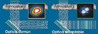
Los MEMS, como toda nueva tecnología, han tenido un impacto importante a la hora de favorecer el acceso a nuevo conocimiento científico. Este es el caso de la llamada óptica adaptable. La luz de los objetos astronómicos que llega a los telescopios terrestres pasa necesariamente a través de la atmósfera, variando su camino óptico por las variaciones de densidad del aire y de temperatura. Como resultado se obtiene una imagen borrosa, con mala resolución angular. Para evitar este problema, una solución costosa es la de ubicar los telescopios en el espacio (como es el caso del Hubble). Otra solución menos costosa e interesante por su capacidad de emplear telescopios grandes, no limitados por las dimensiones que se pueden manejar en los transportes espaciales, es la que aportó el desarrollo de espejos cuya superficie se deforma mediante MEMS, corrigiendo las distorsiones que produce la atmósfera terrestre.

Esquema del dispositivo que corrige las deformaciones de la imagen producidas por la turbulencia de la atmósfera terrestre. La óptica adaptable, realizada mediante MEMS, permite neutralizar este efecto y obtener una resolución angular adecuada como para distinguir objetos estelares que de otra manera se encontrarían confundidos en una imagen borrosa.
Otra aplicación científica de los MEMS fue la realización de instrumentos de medición de fuerzas entre dos objetos cuyas superficies se encuentran a distancias submicrométricas
Adan chaparro
CI:17501640
EES
Direccion WEB:
http://aportes.educ.ar/fisica/nucleo-teorico/estado-del-arte/nuevas-herramientas/dispositivos_mecanicos_ultra_p.php